
BLE 6 Click Board™
Product Code: MIKROE-4170
How Does The BLE 6 Click Board™ Work? The BLE 6 Click Board™ uses the BlueNRG-M2, a Bluetooth low energy application processor module compliant with Bluetooth® v5.0. The BlueNRG-M2 module has been designed around the ST BlueNRG-2 SoC where its Cortex-M0 core can execute both Bluetooth protocols and customer application. Optimized memory architecture includes 256 kB of Flash memory and 24 kB of ultra-low-leakage RAM (with full data retention). A complete power-optimized Bluetooth stack library provides: Master, slave and multiple role support; GAP: central, peripheral, observer or broadcaster roles; Simultaneous advertising and scanning; Capability of being a slave of up to two masters simultaneously; ATT/GATT: client and server; SM: privacy, authentication and authorization; L2CAP; Link Layer: AES-128 encryption and decryption. The BLUENRG-M2 module has both 32 MHz and 32 kHz crystal oscillators implemented. It has been designed to leverage the BlueNRG-2 integrated DC-DC step-down converter in order to achieve the best power consumption in active mode.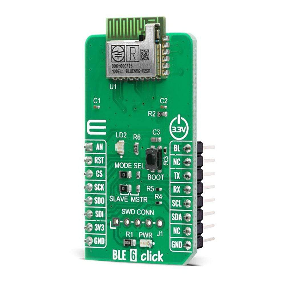
It also embeds a high-efficiency chip antenna. It can be configured to support both application processor (host-less) and network processor (hosted) modes. The BlueNRG-M2 module provides a complete RF application platform in a tiny form factor (11.5 x 13.5 x 2.0 mm) and being a certified solution optimizes the time to market of the final applications. The BlueNRG-M2 module allows applications to meet the tight advisable peak current requirements imposed with the use of standard coin cell batteries.
There are two possible software architectures: Host-less mode (application processor - customer application runs on the BlueNRG-M2 module) and Hosted mode (network processor - the module is configured as network module controlled by an external host connected via SPI or UART). The module comes with a pre-programmed UART bootloader. The BlueNRG-M2 embeds the ARM serial wire debug (SWD) port routed to the SWD header connector. It is two pin (clock and single bi-directional data) debug interface, providing all the debug functionality plus real-time access to system memory without halting the processor or requiring any target resident code. Since the SPI peripheral can be used either as master or slave, the onboard SMD jumpers labeled as MODE SEL allow switching between the two.
The BLE 6 Click Board™ is designed to be operated only with a 3.3V logic level. A proper logic voltage level conversion should be performed before the Click board™ is used with MCUs with logic levels of 5V.
SPECIFICATIONS
Type
BT/BLE
Applications
Internet of Things, Smart Home, Building and industrial automation, Smart Lighting, Remote and access control, Fitness, wellness and sports, Consumer medical, Security and proximity, Assisted living, PC and smartphone peripherals
On-board modules
The BLE 6 Click Board™ uses the BlueNRG-M2 module, a Bluetooth low energy system-on-chip application processor certified module, from STMicroelectronics.
Key Features
High performance, ultra-low power Cortex-M0 32-bit based core, Programmable embedded 256 kB Flash, 24 kB embedded RAM with data retention, Bluetooth v5.0 compliant, Supports master and slave modes, PCB antenna
Interface
Analog,GPIO,I2C,SPI,UART
Compatibility
mikroBUS
Click board size
M (42.9 x 25.4 mm)
Input Voltage
3.3V
PINOUT DIAGRAM
This table shows how the pinout on the BLE 6 Click Board™ corresponds to the pinout on the mikroBUS™ socket (the latter shown in the two middle columns).
Notes
Pin
Pin
Notes
Analog Input
AN
1
AN
PWM
16
BL
Boot
Reset
RST
2
RST
INT
15
NC
SPI Chip Select
CS
3
CS
RX
14
TX
UART TX
SPI Clock
SCK
4
SCK
TX
13
RX
UART RX
SPI Data OUT
SDO
5
MISO
SCL
12
SCL
I2C Clock
SPI Data IN
SDI
6
MOSI
SDA
11
SDA
I2C Data
Power Supply
3.3V
7
3.3V
Visit the Debug Store website for more information on BLE 6 Click Board™
ENQUIRY FORM


